Huawei has formally proposed a paradigm shift in semiconductor engineering designed to transcend the physical and economic boundaries that currently constrain microchip manufacturing.
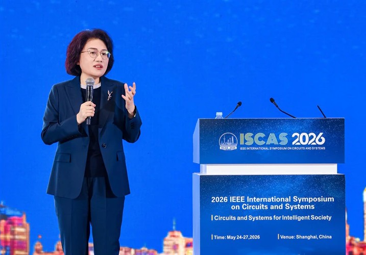
Presenting a keynote address titled “New Semiconductor Path in Practice” at the 2026 IEEE International Symposium on Circuits and Systems (ISCAS), He Tingbo, President of Huawei’s chip design division, introduced the “Tau (τ) Scaling Law.” The theoretical framework advocates for transitioning the industry away from traditional geometric scaling—the continuous physical reduction of transistor dimensions—and adopting time (τ) scaling as the primary benchmark for the evolution of semiconductor architectures and advanced electronic systems.
For more than half a century, Moore’s Law has served as the foundational roadmap for the global semiconductor sector, dictating the predictable doubling of transistor density within a given silicon area. However, as the industry encounters severe sub-nanometer physical limits and diminishing economic returns on cost-per-transistor investments, traditional manufacturing methods have experienced a pronounced deceleration. Huawei’s Tau Scaling framework addresses this critical bottleneck by prioritizing the systematic compression of signal propagation delays, thereby enabling significant advancements in transistor density and processing velocity without relying strictly on lithographic shrinks.
The execution of this methodology relies on a highly integrated, multi-level co-optimization mechanism that simultaneously alters devices, circuits, chips, and broader computing systems. At the micro-layer, engineers target the reduction of resistance and parasitic capacitance within the underlying transistors and physical interconnects to minimize localized delays. Concurrently, at the circuit architecture level, Huawei introduced a proprietary layout framework called “LogicFolding.” This technique circumvents conventional layout boundaries to significantly compress critical-path wiring, thereby mitigating the resistive and capacitive loads that typically impede signal transmission.
This optimization extends upward through the system architecture. At the chip level, the company utilizes a full-stack, coordinated engineering strategy that integrates software, architecture, and silicon substrate design. This framework facilitates precise, workload-driven governance over instruction pipelines and data flows, enhancing structural parallelism and reducing end-to-end execution latency. To scale this performance across massive infrastructure installations, Huawei has deployed a unified interconnect protocol designated as UnifiedBus. The protocol establishes native memory semantics and unified memory addressing for high-density computing clusters (SuperPoDs), minimizing inter-system communication delays.
While conceptually distinct from traditional industry roadmaps, the application of Tau Scaling represents an established operational pipeline rather than a purely academic exercise. Over the past six years, the company has successfully designed and fabricated 381 distinct integrated circuits utilizing these temporal optimization principles across multiple enterprise and consumer sectors.
The initial commercial validation of this architecture is scheduled for Fall 2026, when Huawei’s next-generation Kirin smartphone processors will debut as the first market-ready silicon to integrate the LogicFolding topology. Long-term projections outlined during the symposium indicate that by 2031, high-performance processors engineered under the Tau Scaling Law are expected to achieve a structural transistor density equivalent to a 14 A˚ (1.4 nm) fabrication node.
In concluding the address, Huawei emphasized that resolving the architectural challenges confronting the modern semiconductor landscape necessitates a collaborative international approach. The company noted that the complexity of post-Moore’s Law evolution precludes unilateral solutions, stating an intention to integrate its Tau Scaling methodologies with the ongoing research of global scientists, engineers, and supply chain partners to support the broader stabilization and development of the electronics industry.